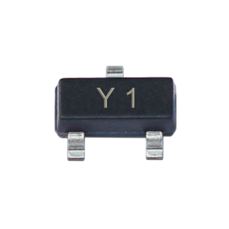
843251AGI-14LF
843251AGI-14LF is a high-performance clock generator or clock buffer chip introduced by Integrated Device Technology (IDT). This type of device is typically used in electronic systems that require high-precision clock signals to ensure timing synchronization and signal integrity.
Application Scenarios:
- Communication Equipment:
- Network devices like routers, switches, and base stations.
- Fiber-optic communication and high-speed data transmission systems.
- Data Centers:
- Servers, storage devices, and network interface cards (NICs).
- Industrial Equipment:
- Industrial automation control systems and PLCs (Programmable Logic Controllers).
- Consumer Electronics:
- High-end TVs, set-top boxes, and gaming consoles.
- Test and Measurement Equipment:
- Oscilloscopes, signal generators, and spectrum analyzers.
Key Parameters:
1. Clock Characteristics
- Output Frequency Range: Typically supports frequencies ranging from tens of MHz to hundreds of MHz (specific range depends on the model).
- Output Types: Supports differential clock outputs (e.g., LVDS, LVPECL, HCSL) or single-ended clock outputs (e.g., LVCMOS).
- Number of Outputs: Usually provides multiple clock output channels (e.g., 4, 8, or more).
- Jitter Performance: Features extremely low phase jitter, typically in the range of a few hundred femtoseconds (fs), suitable for high-speed communication systems.
2. Input Characteristics
- Clock Source: Supports external crystal oscillators, clock signals, or reference clock inputs.
- Input Voltage Range: Typically compatible with 1.8V, 2.5V, or 3.3V logic levels.
3. Power Characteristics
- Operating Voltage: Typically 3.3V or 2.5V.
- Power Consumption: Low-power design, suitable for energy-efficient applications.
4. Package
- Package Type: Usually small-sized surface-mount packages (e.g., QFN or TSSOP).
- Pin Count: For example, 14 pins (specific count depends on the model).
5. Operating Temperature Range
- Industrial Temperature Range: -40°C to +85°C, suitable for industrial environments.
Typical Application Circuit:
- Clock Input: External crystal oscillator or reference clock signal.
- Clock Output: Connected to devices requiring synchronized clock signals (e.g., FPGAs, ASICs, processors).
- Power Decoupling: Decoupling capacitors are added near the power pins to reduce noise.
- Configuration Pins: Used to set output frequency, division ratio, or other parameters.
Advantages:
- High Precision: Provides low-jitter clock signals, ensuring accurate system timing.
- Flexibility: Supports multiple output types and frequency configurations to meet diverse application needs.
- Low Power Consumption: Suitable for power-sensitive devices.
- High Reliability: Industrial-grade design, suitable for harsh working environments.
Welcome to consult!


